- +1 437-291-8881
- pcb@qualiecocircuits.ca
Learn about printed circuit board and stencil technology and empower your business!
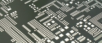
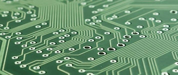
PCB Technology
Glossary and Abbreviations - PCB Glossary
Click on an alphabet below to directly jump to the chosen alphabet section...
ABCDEFGHIJKLMNOPQRSTUVWXYZAlphabet D
- DatabaseA collection of interrelated data items stored together without unnecessary redundancy, to serve one or more applications.
- Date CodeMarking of products to indicate their date of manufacture. ACI standard is WWYY (weekweekyearyear).
- DatumThe theoretically: exact point, axis or plane that is the origin from which the location of geometric characteristics of features of a part are established.
- DelaminationA separation between plies within a base material, between a base material and a conductive foil, or any other planner separation with a printed board.
- Design Rule CheckingThe use of a computer: aided program to perform continuity verification of all conductors routing in accordance with appropriate design rules.
- DesmearThe removal of friction melted resin and drilling debris from a hole wall. Destructive testing: Sectioning a portion of printed circuit panel and examining the sections with a microscope. This is performed on coupons, not the funtional part of the PCB.
- DewettingA condition that results when molten solder has coated a surface and then receded. It leaves irregularly shaped mounds separated by areas of thin solder. The base material is not exposed.
- DFSMDry Film Solder Mask.
- DieIntegrated circuit chip as diced or cut from a finished wafer.
- Die BonderThe placement machine bonding IC chips onto a chip on board substrate.
- Die BondingThe attachment of an IC chip to a substrate.
- Dimensional StabilityA measure of the dimensional change of a material that is caused by factors such as temperature changes, humidity changes, chemical treatment, and stress exposure.
- Dimensioned HoleA hole in a printed board whose location is determined by physical dimensions or coordinate values that do not necessarily coincide with the stated grid.
- DoubleSidePCBThe PCB having two circuit layers with pads & traces are on both sides of the board. Double sided Laminate: A bare PCB laminate having tracks on both sides, normally PTH holes connecting circuitry two sides together.
- Double side component assemblyMounting component on both sides of PCB, for e.g. SMD technology.
- DrillToolDescriptionThis is a text file describing drill tool number and corresponding size. Some reports also include quantity. Please Note: All drill sizes will be interpreted as plated through finished sizes unless otherwise specified.
- DrillFileIn order to process your order, we require a drill file (with x:y coordinates) that is viewable in any text editor.
- Dry Film ResistsCoated photosensitive film on the copper foil of PCB using photographic methods. They are resistant to electroplating and etching processes in the manufacturing process of PCB.
- Dry Film Solder MaskA solder mask film applied to a printed board using photographic methods. This method can manage the higher resolution required for fine line design and surface mount.
PCB Design Tips
When designing a PCB, try to limit the amount of draws you use. Draws use a lot of memory and slow the programming time. Use a flash for pads instead.
More tips...
Contract Assembly
We are one-stop solution provider for all your contract assembly requirements. We have the capability and resources to provide PCB assemblies, as well as cable and harness assemblies.
What our customers say?
QualiEco Circuits Limited is an excellent supplier to us! We appreciate the quality of service and support that we receive from QualiEco Circuits. They always deliver what is promised
For printed circuit boards (PCBs) or PCB assembly you can count on. Email to the friendly and experienced team at QualiEco Circuits, Canada.